Dislocation Nucleation in Si
Faculty Participants
Catalin Picu
Professor
Current and Former Students
Zhi Li
Graduate Research Assistant
Description
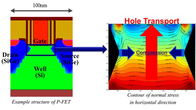
Stress improves semiconductor device performance by improving carrier transport. Dual stress liners (DSL) are commonly incorporated into device designs to improve both electron andhole transport. Embedded SiGe is added to PFET’s design to create additional strain in the channel for even better PFET performance. However, large stress fields can cause dislocation nucleation, leading to increased leakage currents or shorts. Dislocations form from stress concentrator sites such as re-entrant corners and joints of dissimilar materials, which are abundant in devices. Furthermore, complex SiGe domain geometries introduce stress states which may or may not be well predicted using current continuum modeling methods. The stress state induced by SiGe layers is essential in the function of current and future devices and it should be insured that this field does not lead to damage nucleation.
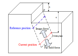
We have studied the nucleation of dislocations from stress concentration sites with idealized geometries using atomistic models. Both pure Si and Si-x%Ge models have been considered. The fraction of Ge in Si, x, was kept as a parameter. Figure 2 shows the geometry of one of the models considered. The stress close to the re-entrant corner is much larger than elsewhere and drives defect nucleation from the corner. Once nucleated, the defect is under the action of another force, the “image force” which pulls the dislocation back to the surface. As the dislocation moves into the material, both image and driving force decrease.
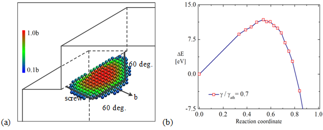
As the nucleus of a new dislocation forms, the energy goes up (driving force does work against the image force). When the nucleus becomes large enough, the energy reaches a maximum and then decreases. This maximum energy is called the activation energy for nucleation and the configuration corresponding to this state is the critical nucleus. Figure 3 shows the critical nucleus forming next to the corner and the variation of the energy with during the defect nucleation process. The activation energy for nucleation is approximately 11eV. This indicates that in order to force the nucleation of a dislocation, increasing the temperature is insufficient and one has to apply a large stress.
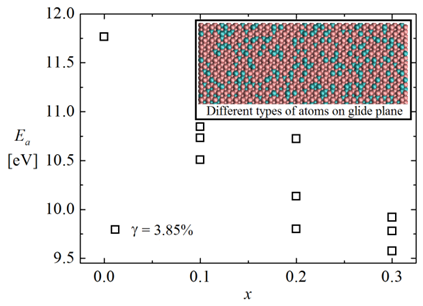
In presence of Ge (i.e. in substitutional alloys of Si-x%Ge), the situation is similar, but the activation energy for nucleation decreases. Figure 4 shows the variation of this parameter with the Ge concentration, x. As x increases up to 30%Ge, the activation energy decreases by approximately 20%, which is a non-negligible effect.