Scientific modeling and simulation are baked into the foundations of the microelectronics industry. Electrical behavior and characteristics of every type of passive and active device are explored with physically-based simulation at the very start of the development process; sophisticated software and algorithms sit in the inner loop of the circuit design workflow with entire layouts being generated and checked by computer; new manufacturing processes are developed and optimized using simulation software; computational logistics and reliability analyses come into the manufacturing process at every level. Just as Moore’s Law has driven other parts of that workflow forward, simulation and modeling technologies have had to constantly progress to keep up. At the Scientific Computation Research Center, we have a long history of working with industrial partners in microelectronics to move the state of the art forward.
Primary Contact: Max Bloomfield
SCOREC Researchers: Bloomfield, Merson, Maniatty
External collaborators: USC, IBM
Microelectronics Modeling Developments
Applications include:
- Bayesian machine learning for advanced patterning
- Physics and chemistry-based reactive ion etch with ballistic transport
- Thermomechanical response of EUV pellicles
- Nonlinear creep in large arrays of C4 joints
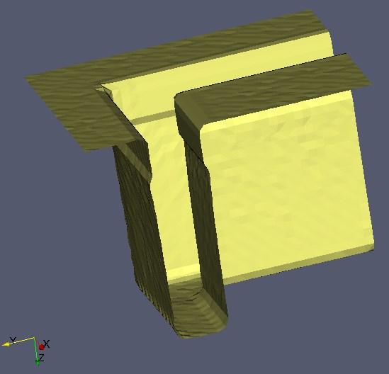
- Laser grooving for die singulation
Bayesian machine learning
We used stochastic neural network techniques to model the behavior and variability of the self-aligned quadruple patterning process used for manufacturing FINFET. We showed how real predictions can be made early in the processes, trading process certainty for timely knowledge. Bloomfield, et al, JM3, 21(4) 2022, https://doi.org/10.1117/1.JMM.21.4.041604
Collaborators: IBM

Thermomechanical response of EUV pellicles
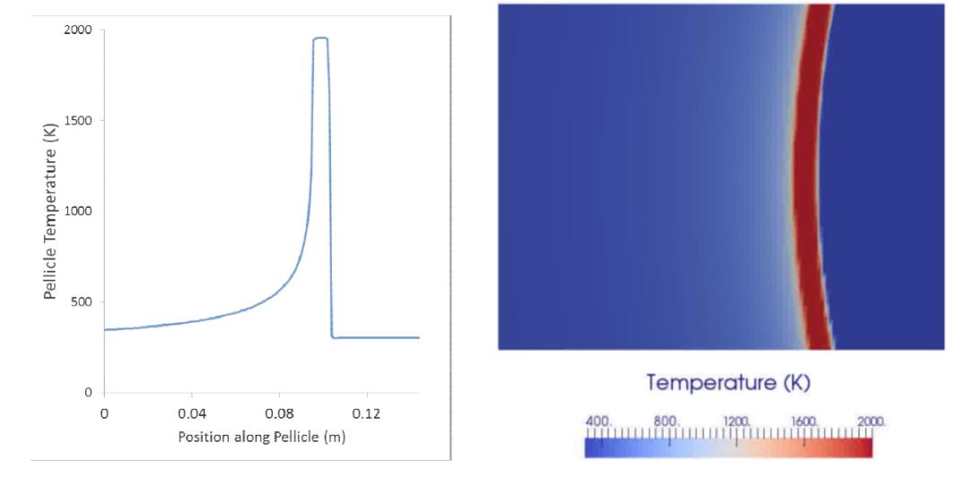
EUV scanners expose in a slit window for manufacturing reasons, scanning across the mask and the wafer die simultaneously. Any intervening pellicle must be thermomechanically stable with the heterogenous heating due to the localized exposure. The ultrathin (10nm) freestanding pellicle cools via Boltzmann radiation throughout its thickness. The temperature gradients can cause wrinkling if expansion locally overcomes pre-stressed state.
Goldfarb et al, Proc. SPIE 9776, Extreme Ultraviolet (EUV) Lithography VII
Collaborators: IBM
Bloomfield, et al, JM3, 21(4) 2022, https://doi.org/10.1117/1.JMM.21.4.041604
Goldfarb et al, Proc. SPIE 9776, Extreme Ultraviolet (EUV) Lithography VII
Hu, et al. ASME2020 doi://10.1115/MSEC2020-8319
Li, et al., Comput. Mech., 62 (3), 2018
Bloomfield, et al., Eng. with Comp. 33, 2017.
Laser grooving simulation
Die singulation can be aided by laser grooving a kerf through multi-material stacks. We simulated the material removal and the interaction with the heterogenous substrate. Hu, et al. ASME2020 doi://10.1115/MSEC2020-8319
Collaborators: IBM
Nonlinear creep/plastic response of large solder joint arrays
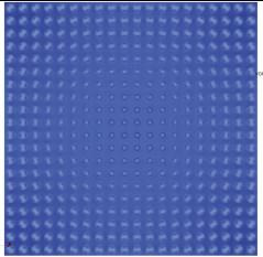
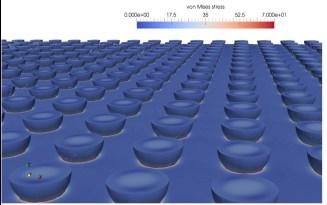
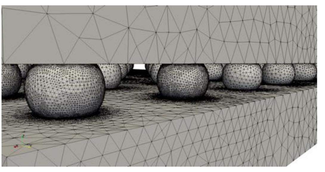
Arrays of thousands of controlled collapse chip connection (C4) solder balls are subject to thermocycling stresses during and after manufacture. Nonlinear plastic responses within each C4 can vary widely over entire arrays. We automated the process of simulating very large arrays with tens of millions of finite elements on HPC systems using novel thermomechanical models. Li, et al., Comput. Mech., 62 (3), 2018; Bloomfield, et al., Eng. with Comp. 33, 2017.
Collaborators: IBM
3D ballistic transport and reaction models of reactive ion etching
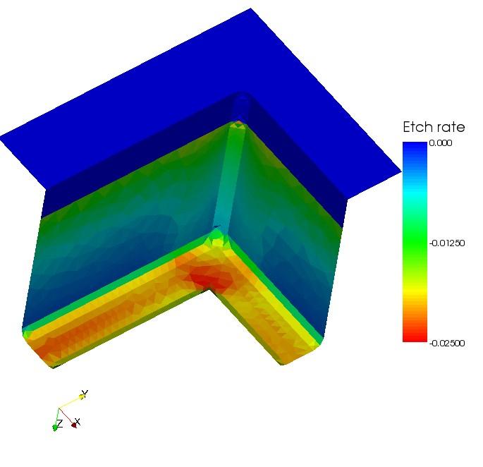
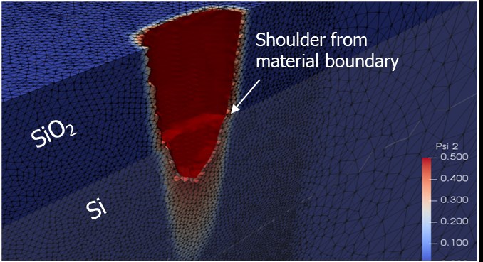
RIE is the most important process technology for pattern transfer to the wafer. We model the transport of ionic and neutral species from an industrial plasma and through a lithographic mask and the reaction rates of those species at the surface to etch the wafer, updating the resulting 3D surface shape and chemistry throughout.
Collaborators: IBM


