Computational Methods Research
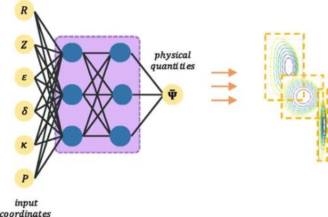
AI/ML techniques are playing an increasing role in scientific computing, capturing, predicting, and providing insight into the behavior of highly complex systems. Deterministic and stochastic neural network, and agent-based approaches are being developed to analyze the responses of a wide variety of computationally difficult problems.
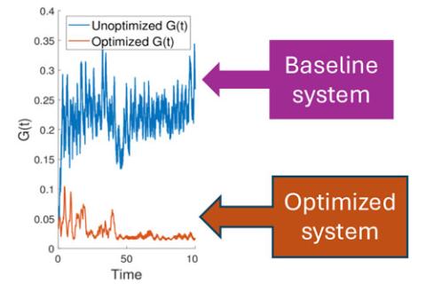
High-fidelity design optimization procedures that employ high-fidelity simulations and advanced optimization methods are required to reliably design many of today’s engineered systems which are governed by complex, nonlinear behaviors.
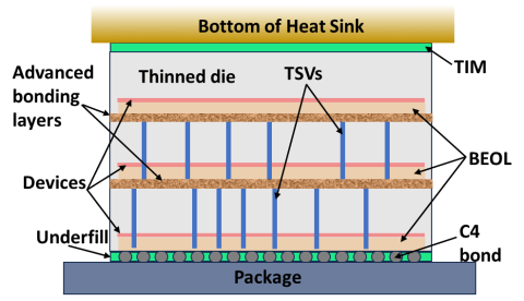
The behavior of many important problems of interest are controlled by interactions across multiple physical and temporal scales. Methods and tools to support the simulation of multiscale problems and to couple the codes that simulate the behavior at the various scales are under development.
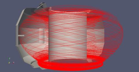
Unstructured mesh particle methods are highly effective when the geometry is complex and/or the distribution of particles is not uniform. An infrastructure to support unstructured mesh particle simulations on massively parallel heterogeneous computers is under development.
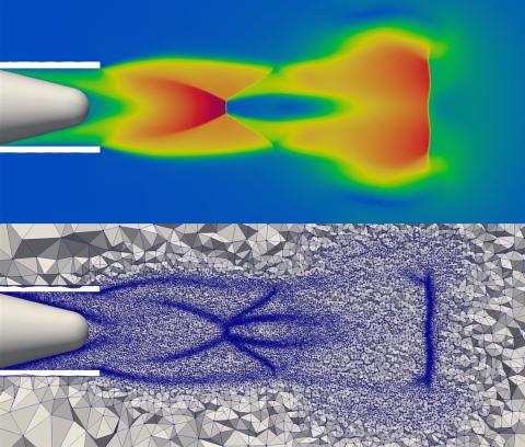
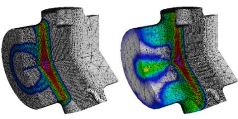
Unstructured meshes support automated simulations over general geometric domains. By providing an infrastructure for operation on, and modification of, unstructured meshes on massively parallel heterogeneous computers, the complexity of developing unstructured mesh-based simulation codes is dramatically reduced.
Effective PDE discretization methods are available for many applications, but there is a continuing need for new methods to solve the most challenging sets of PDEs and to provide automated simulation workflows that adaptively control these discretizations to ensure the accuracy of the numerical solutions.

As evidence of quantum utility mounts, efforts are underway to develop hybrid quantum high performance computing methods to realize quantum advantage using today's noisy cubits.